I've been working on a large project for a few months now. It's a DC power distribution unit, and as you can imagine it has need for relays. I've got the thing setup to accept cards to can perform many uses both input and output. One of the many cards I've designed for this system (dual low-side switching relay, 5V, 12V, audio sensor etc..) is a dual high-speed 12V solid state relay card.
This is a photo of the relay on a breadboard.
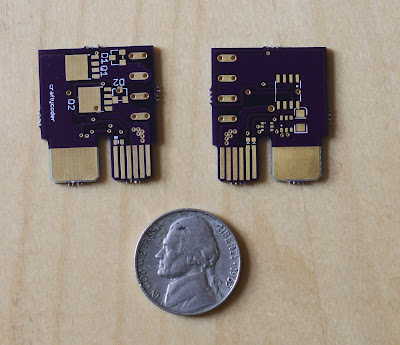
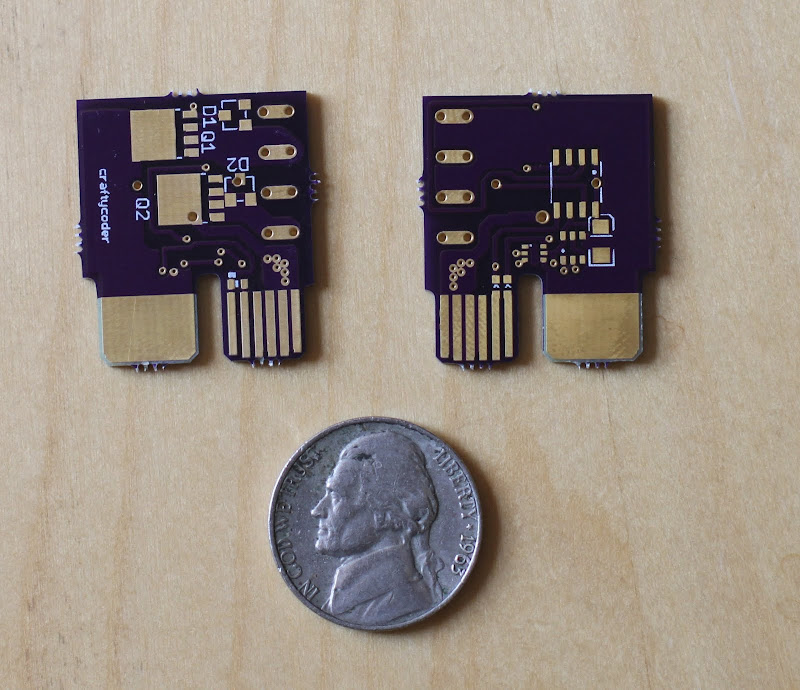
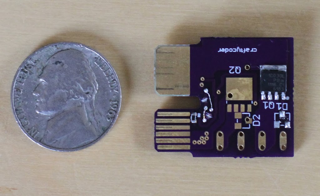
This is the card from both sides. The "empty" space is used for thick and wide traces to carry current. These will be built with 6oz copper and can source 23A @ 330W in theory. I've only pushed them to 100W so far but they showed no meaningful rise in temperature so I think I am on the right track. By the numbers, they are right where they should be.

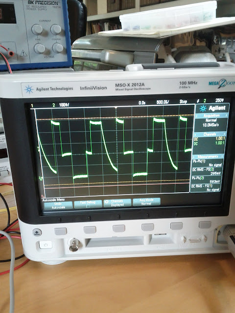
Not so square... :(
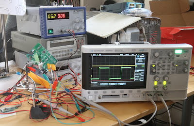
I began going through everything and I found the problem, but what to do? Well, run new wires of course!


|
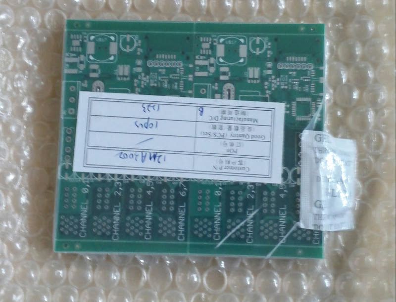
| Rendering of PDU and fresh pile of PCBs from Circuitmart |
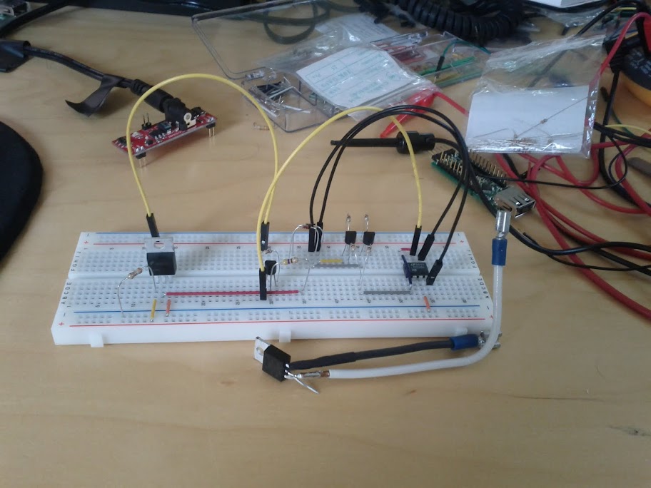 |
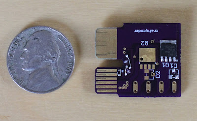
| single channel of dual high-speed 12V solid state relay on breadboard |
Because these cards are small and parts count it large (4 diodes, 6 transistors, a driver IC, 7 resistors, 1 tant cap) I sourced ICs with the configs I needed inside of them pre-configured. You would be amazed what you can find at Digikey if you look hard enough. Anyway, I'd never used these ICs before so I was required to design the footprints for them and lay them all out and what not. Long story short (too late), I read the datasheet wrong for one of them and got some pins confused. I didn't notice this until I had it all built up and my beautiful square wave looked like this.
I began going through everything and I found the problem, but what to do? Well, run new wires of course!
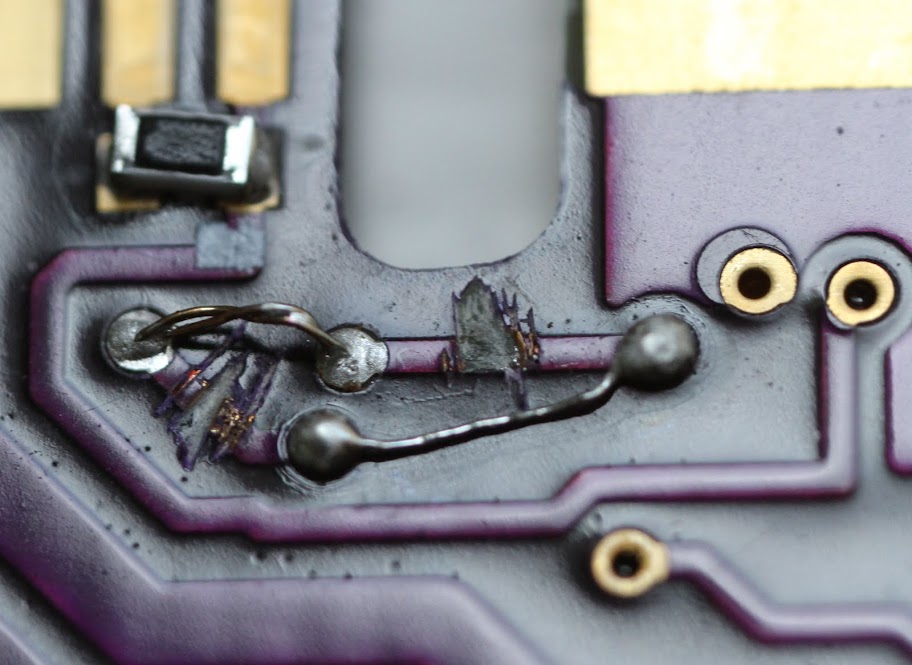
I didn't have to do any drilling because I happened to have vias available so I just needed to cut some traces and thread some wire. I used an old length of stranded telephone wire. After stripping the outer shield, I removed one of the four insulated wires inside and stripped it down to its constituent 8 strands. I used two strands (twisted) for the short trace and one strand of the longer one. In order to raise the single strand's current capacity a bit, I wet the entire length of the strand with solder. This also stiffens it so it wont bend so easy.
My square waves have returned to me!

Comments
Post a Comment